This tutorial is adapted from Instructables website.
Overview, Datasheet, Dimensions
In this tutorial, we will create a new component for use in Eagle CAD.
In Eagle, each component is defined by three items:
-
a package - the footprint of the component on the PC board.
-
a symbol - the component’s symbol used when laying out the schematic diagram for a circuit.
-
a device - a package and symbol, connected together and ready for use in your design.
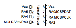
The component we’ve chosen for this tutorial, the PIC12F1822, is an 8-pin, 8-bit microcontroller.
First, take a look at the data sheet.


Note that all dimensions are specified in inches.
To create the package (i.e., the footprint), we’ll need to lay out pads at the right location for each of the eight legs. The key dimensions for laying out the pads are these:
-
Pitch (the distance between the leads) “e”: 0.1
-
Shoulder to shoulder width “E”: 0.31
-
Lower lead width “b”: 0.018
-
Lead thickness “c”: 0.01
Later, when we create the package, we’ll need this dimension for laying out the physical component:
-
Overall length “D”: 0.365
Step One: Creating the Package (the Footprint)
Open EagleCad
Go to File > New > Library
We’ll be creating a package, so click on package icon.

In the New field, type PIC12F1822 and click OK. Click OK again if you get a warning asking “Create new package”.
Setting the Pad Dimensions
Let’s set the size of the pads that we’ll need. Looking at the dimensions, we see that the leads are 0.01 x 0.018. So let’s set the holes in the pads to the larger of those dimensions: 0.018. Given this, a good size for the pads overall is 0.03.
To set those dimensions into Eagle CAD, click on the pad icon
Change the shape and dimension of the the pad, as shown in the illustration below.
![]()
Laying Out the Pads
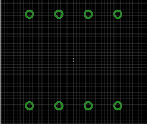
The cross is the center of our package is the origin of Eagle’s coordinate system. Our package has eight legs placed symmetrically about the center, four above the midline and four below. Let’s calculate the placement of the one of the legs in the lower row, the second from the right. Its x-coordinate is 0.05 -- one half of the distance between the legs (“e” = 0.1). Its y-coordinate is -0.155 -- one half the shoulder to shoulder width (“E” = 0.31).
Note that the finest precision we need is 0.005, needed for the y-coordinate, so set the grid to 0.005 as follows:
Click on the grid icon or type in “grid” in command to change the grid size.

Now set grid size to 0.005. Check to be sure the units are set to inches, then click OK.
(You might not see the grid on your screen, depending on how much zoom you’re using.)
Place the first pad by clicking again on the pad symbol and moving your cursor to the x and y coordinates we calculated above. (You may have to adjust the zoom to get in the right range.) The position of the cursor is shown at the top left of the layout area. When your cursor is in the right position, the readout will show “0.005 inch (0.05 -0.155)”. When you’re at the right position, left-click to place the pad. If you have trouble positioning a pad this way, just right click on the pad, choose “Properties”, and set the coordinates manually on the second line of the dialog box (“Position”) .
Calculate the x-coordinates of the other pads in the lower row by adding or subtracting the Pitch (0.1), and place the pads using the same technique. Since we know the legs are symmetric around the center, the coordinates in the upper row are the same as the lower, with the y-coordinate changed from negative to plus.
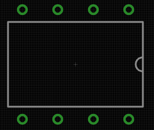
Here is the result after adding pads
At this point, it would be wise to save your work. Click on the Save icon and name your new library. Save frequently as you work.
Drawing a Shape to Represent the Package
The next step is drawing a shape to represent the package on the silkscreen layer of the board; the exact dimensions are not critical. We’ll want a shape about as long as the package (Overall length “D”: 0.365) and somewhat narrower than the spacing between the pads. We don’t want the lines to overlap the pads, because the silkscreen ink would cover the copper of the pads. To draw the shape, use the Drawing Tool called Wire, accessed either from the icons at the left, or the Draw menu. Use the drawing tool called Arc to draw the chip orientation symbol at the right.
As you are drawing, note that the tool defaults to the Layer 21 (tPlace, the silkscreen layer).

Here is the result.
Naming the Pads
Next, we will name each of the pads with the names set out in the specification.
Here’s how to do it. Click on the name icon at the left, or find it in the Edit menu, or type “name” in the command line. Then click on each pad and enter the appropriate name.
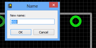
Here’s the result

Step Two: Creating the Symbol
Click on the symbol icon
Enter the name (PIC12F1822) and click OK. Click Ok again if you get a warning.
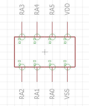
Click on the “Draw wires” icon to create a rectangle about 0.8 x 0.4. Make it symmetric around the center cross.
Next, start the Pin tool by clicking on the icon at the left, or typing “pin” in the command line, or finding it in the Draw menu. Note that a new toolbar appears at the top. To rotate the pin, right click before placing the pin with a left click. Place eight pins.
Next, change the name of the pins to match the pad names. Do this by using the Name tool again and clicking on the circle part of the pin.
Here’s the result.
Step Three: Create a device
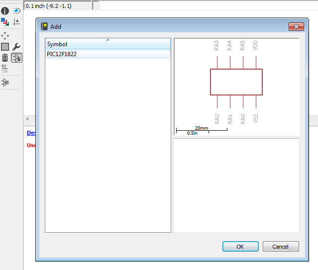
Click on device icon
Type the same name again (PIC12F1822), and click OK.
At the bottom of the screen, click New and select the package you created. Then click OK.

On the left toolbar, click the Add icon and choose the symbol you just created.
Click OK. Move the cursor to the upper left panel and left click to place the symbol. Move it so that the little cross in the center of the symbol is on top of the cross in the center of the panel. An easy way to do this is to right click on the symbol’s cross, choose Properties, set the Position to 0, 0, and click OK.

Now, we’ll match up the pins on the symbol to the pads on the package.
Click on Connect at the bottom right and you’ll be presented with this screen
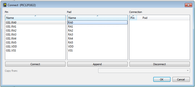
Note that the first line is highlighted. If the matchup is correct, click Connect. If not, match the pad to the correct pin and then click Connect. Do this for each pin. You’ll end up with this.
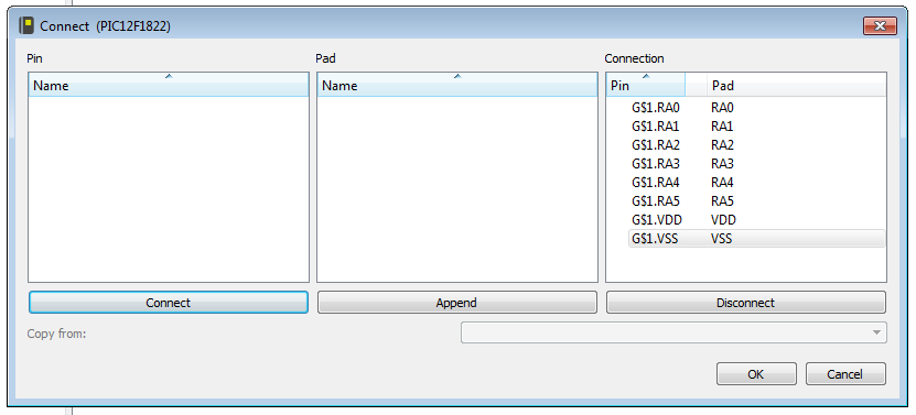
Click OK, then click Save. You’ve successfully completed your first Eagle component.